How Are Solid State Drives Made From Silicon to Finished Storage?
Explore the materials, manufacturing stages, firmware, and testing behind modern SSDs
-
SSDs combine NAND flash memory, controllers, firmware, and printed circuit boards made from purified silicon wafers.
-
Their lack of moving parts delivers faster access, lower power use, and better durability than traditional hard drives.
-
Manufacturing includes wafer fabrication, photolithography, die assembly, firmware programming, and rigorous burn-in testing.
A modern solid-state drive is the result of several highly specialized manufacturing processes. It starts with ultrapure silicon and ends with a compact device that can store terabytes of files without using spinning disks or moving heads. Semiconductor factories create the memory dies, electronics manufacturers assemble the controller and circuit board, and software teams program the firmware that coordinates every operation. Companies such as Kingston Technology and Sandisk sell finished SSDs, while different suppliers may manufacture the memory, controller, and enclosure. Understanding how these parts are made helps explain why SSDs are fast, durable, and sensitive to heat, wear, and manufacturing quality.

What Is a Solid-State Drive and How Does It Work?
Definition and key attributes
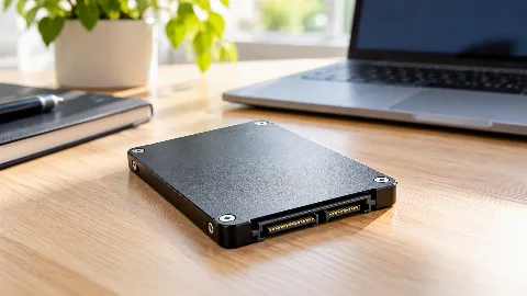
A solid-state drive stores data electronically rather than magnetically. It uses semiconductor memory to preserve information even when power is removed. An SSD has no spinning platter, actuator arm, or read and write head. That design gives it low access latency, quiet operation, resistance to vibration, and lower energy use. SSD performance varies by interface, memory type, controller design, and workload. A PCIe NVMe drive can handle far more parallel requests than an older SATA model, while an M.2 device describes a small physical form factor rather than a specific speed.
Comparison with traditional hard drives
Traditional hard disk drives use rotating magnetic platters and mechanical heads. The drive must wait for a platter to rotate and a head to move into position, creating mechanical latency. SSDs access electronic memory directly, so they usually start applications and retrieve small files much faster. Hard drives can still offer a lower cost per terabyte, especially for archival capacity, but SSDs generally provide stronger shock resistance and more consistent responsiveness.
Basic architecture and components
An SSD typically includes NAND memory packages, a controller, temporary DRAM or a host-memory buffer, power management components, and a circuit board. The controller translates computer commands into memory operations, manages error correction, and spreads writes across available cells. An enclosure protects the assembly and helps regulate heat. Enterprise models may add capacitors that preserve in-flight data during a power interruption.
What Materials Are Used to Make SSDs?
Silicon wafers and their preparation
The central raw material is ultrapure silicon, formed into thin silicon wafers. Manufacturers polish each wafer until its surface is extremely flat, then deposit and pattern layers that become transistors and wiring. The wafer itself does not become a complete SSD. Instead, it holds many repeated memory and logic designs that are later separated into individual dies.
NAND flash memory technology
NAND flash memory provides the nonvolatile storage capacity. NAND uses arrays of electronic cells that retain charge after power is removed. Single-level cell stores one bit per cell, while multi-level cell, triple-level cell, and quad-level cell store progressively more bits. Higher density reduces cost, but it also requires more precise voltage control and stronger error correction. NAND is different from technologies such as 3D XPoint, which used a separate class of persistent memory architecture.
Other components: controllers, PCBs, connectors
The controller is a specialized processor that coordinates host communication, flash translation, error correction, encryption, garbage collection, and wear leveling. A printed circuit board connects the controller, memory packages, power circuitry, and interface contacts. The board is usually made from fiberglass reinforced with epoxy resin and copper traces. Connectors depend on the product design, including SATA cables, PCIe edge contacts, or the compact contacts used by M.2 drives. Capacitors, resistors, voltage regulators, and thermal materials complete the electronic assembly.
How Are Silicon Wafers Made and Processed?
The Czochralski process for silicon crystal growth
Wafer production begins by refining quartz-derived silicon until impurities reach extremely low levels. In the Czochralski Process, a small seed crystal is dipped into molten silicon and slowly pulled upward while rotating. The silicon solidifies around the seed, producing a large cylindrical single crystal called an ingot. Engineers control temperature, pulling speed, rotation, and dopant concentration to create the electrical properties required for semiconductor manufacturing.
Photolithography and wafer fabrication
After the ingot is sliced into wafers, manufacturers grind, polish, clean, and inspect the surfaces. The wafers then enter a cleanroom for repeated patterning steps. Photolithography coats a wafer with light-sensitive photoresist, exposes it through a patterned mask, and develops the resist to reveal selected areas. Etching removes material, deposition adds insulating or conducting films, and ion implantation changes the electrical behavior of specific regions. Repeating these steps creates transistors, insulating layers, and microscopic connections. The result is a wafer containing thousands of complex integrated circuits, depending on die size.
Testing and sorting silicon wafers
Automated inspection systems search for particles, scratches, pattern defects, and dimensional errors. Electrical probes test selected structures on each wafer to identify working and marginal dies. Mapping software records the position of failures so later cutting and assembly equipment can separate good dies from defective ones. Manufacturers sort parts by performance, voltage behavior, and expected endurance. This screening is essential because a tiny defect in one layer can make a memory die unreliable.
What Is the NAND Flash Fabrication Process?
Creating memory cells with microscopic transistors
NAND fabrication builds an array of charge-storing structures connected through word lines and bit lines. Each memory cells stores an electrical charge at a controlled level. The charge changes the transistor's threshold voltage, and the controller later interprets that voltage as a data state. Fabrication adds insulating films, conductive gates, channel structures, and contacts in carefully aligned layers. The process must control contamination and thickness at microscopic scales because small variations affect voltage ranges and endurance.
3D NAND technology and its advantages
3D NAND stacks memory layers vertically instead of placing every cell only across a flat surface. Manufacturers build a tall structure, form vertical channels through it, and connect the layers into a working array. More layers increase capacity within a small footprint and can reduce the need for extremely aggressive horizontal scaling. Modern 3D NAND may use hundreds of layers, although the exact count depends on the supplier and product generation. Vertical construction also creates challenges involving alignment, channel uniformity, manufacturing time, and heat management.
Die assembly and packaging
Once wafer testing is complete, a diamond saw or laser separates individual dies. Die assembly attaches working memory dies to a package substrate and connects them through wire bonds or microscopic bumps. The package receives protective materials and electrical contacts before inspection. Packaging determines how many dies can fit on a module, how heat leaves the device, and how the finished memory connects to the SSD board. Multiple NAND dies may share one package to increase capacity and parallelism.
How Is Firmware Developed and Programmed in SSDs?
Role of firmware in SSD functionality
Firmware is the embedded software that makes an SSD usable. It translates commands from the operating system into NAND operations, maintains the flash translation layer, and tracks where logical data resides on physical memory. It also controls error correction, bad block management, wear leveling, garbage collection, encryption, thermal limits, and power states. Without firmware, the memory chips would not present a reliable storage interface to a computer.
Programming and initialization steps
Engineers first develop and validate firmware against a specific controller, NAND generation, interface, and product configuration. During production, a programming station loads the approved firmware image into nonvolatile controller memory or another designated storage area. The drive then runs initialization routines that identify installed NAND, create translation tables, reserve spare blocks, set operating parameters, and verify communication with every memory package.
Manufacturers may program different firmware versions for consumer, workstation, and data center models. The software is tested with operating systems, motherboard interfaces, power transitions, queue depths, and unusual error conditions. A final configuration step records the model number, capacity, serial number, security settings, and calibration data. Vendors such as Kingston Technology and Sandisk can later distribute firmware updates that fix bugs, improve compatibility, or adjust performance and endurance behavior.
What Quality Assurance Steps Ensure SSD Reliability?
Burn-in testing and final inspection
Quality assurance begins with inspection of incoming wafers, packages, boards, and electronic components. After assembly, automated testers confirm capacity, interface behavior, power consumption, temperature response, and sequential and random performance. Burn-in testing runs drives under sustained read and write workloads, often at elevated temperature or voltage conditions within safe limits. This process can expose early-life failures before products reach customers. Final inspection checks solder joints, labels, connectors, enclosure fit, firmware identity, and mechanical damage.
Reliability metrics and endurance considerations
Manufacturers evaluate an SSD using metrics such as terabytes written, drive writes per day, uncorrectable bit error rate, mean time between failures, and data retention. These figures are estimates based on memory type, workload, temperature, and firmware behavior rather than guarantees that every drive will fail at a particular point. Testing also measures how well error correction recovers weakened signals and how effectively wear leveling distributes writes.
Endurance is influenced by the number of bits stored in each cell. Higher-density NAND can experience narrower voltage margins, so the controller relies on stronger error correction and background maintenance. Temperature matters too. Excess heat can accelerate wear and reduce retention, while very low temperatures may affect programming speed. A well-designed SSD combines robust components, conservative firmware settings, spare capacity, and thorough production screening.
How Do SSDs Store and Retrieve Data?
Memory cell operation and data encoding
Data storage in NAND begins when the SSD applies carefully controlled voltages to program a cell. Electrons become trapped in an insulating layer, shifting the transistor's threshold voltage. To read the cell, the NAND circuitry applies test voltages and measures whether current flows. In single-level cell NAND, two voltage states represent one bit. Multi-level designs use several voltage ranges, allowing one cell to represent multiple bits but leaving less separation between valid states.
Controller algorithms and data management
The controller presents logical block addresses to the computer while privately mapping them to physical NAND locations. This mapping is necessary because NAND cannot overwrite data in place. The controller writes updated data to a new location, marks the old location invalid, and later combines valid pages during garbage collection. Wear leveling moves data so the same cells are not repeatedly programmed. Error correction codes detect and repair many bit errors, while read retry and voltage calibration help recover data as cells age.
When you delete a file, the operating system may send a TRIM command. The SSD uses that information to identify pages that no longer contain useful data, which makes future garbage collection more efficient. Parallel NAND channels allow several packages to work at once, increasing throughput. The controller also manages caching, encryption, thermal throttling, and power loss behavior. Together, these hardware and software systems turn slow, complex cell-level operations into the familiar storage device shown by your computer.
Making an SSD requires much more than placing memory chips on a circuit board. Semiconductor engineers grow and pattern silicon, NAND specialists create dense vertical memory structures, and electronics teams assemble, program, and test the finished drive. The controller and firmware determine how effectively the device manages wear, errors, heat, and performance. When you compare SSDs, look beyond advertised speed. Check the NAND type, interface, endurance rating, warranty, thermal design, and firmware support. Those details reveal how the manufacturing choices will affect your everyday use.
How long does it take to manufacture an SSD?
The semiconductor portion can take several weeks because wafer fabrication involves hundreds of controlled steps. Die assembly, board production, firmware programming, testing, and shipping add more time before a finished SSD reaches customers.
Are SSDs made from silicon?
Yes. The NAND memory and controller are built from semiconductor materials based primarily on purified silicon. Silicon is formed into wafers, processed into circuits, cut into dies, and packaged into the components used in an SSD.
What is the most important part of an SSD?
NAND flash provides the storage capacity, but the controller and firmware strongly influence speed, endurance, error handling, and reliability. An SSD performs well only when these parts work together.
What is the difference between 2D NAND and 3D NAND?
2D NAND places cells across a mostly flat surface, while 3D NAND stacks cell layers vertically. 3D NAND can provide greater capacity and improved density in a compact package, although it requires more complex fabrication.
Do SSDs have moving parts?
No. SSDs use electronic memory and contain no spinning platters or moving read and write heads. That is why they are generally quieter, faster for random access, and more resistant to physical shock than hard disk drives.
How are SSDs tested for reliability?
Manufacturers inspect components, test electrical behavior, verify capacity and performance, and run sustained workloads during burn-in testing. They also evaluate endurance, error rates, temperature response, data retention, and firmware behavior.